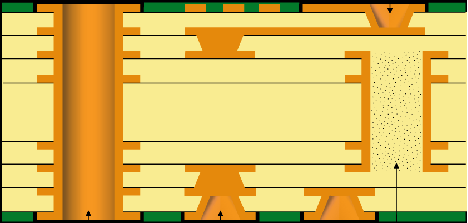
Metallization are important processes for 3D IC chip packaging and printed circuit board (PCB) fabrication
For PCB with high density interconnection, microvia and Through Hole (TH) filling with copper deposit become more and more important, especially for smart phones. Both microvia and TH are composed of resin and glass fiber, which means that they are not conductors.
The metallization processes include dry and wet processes. Usually, dry processes, such as PVD, CVD and sputtering, are employed for the IC packaging fabrication whereas wet processes, such as electroless deposition and coating of conducting material, are employed for PCB fabrication. No matter dry or wet process, conductive seed layer is essential for sidewall metallization. A new metallization process proposed is using graphene as the seed layer.
Through Hole (TH) Microvia Microvia
Graphene Direct Metallization Process is a patented graphene based dispersion of conductive colloids used to make conductive for subsequent copper plating on various kinds of substrate materials. Most suitable for HDI and Flex PCB. ‧ Better conductivity than Graphite ‧ Formaldehyde free and reduced water usage ‧ Superior Reliability ‧ Copper-to-copper direct bonding strength and good reliability ‧ No chelating agents and heavy metals. ‧ Simple, easy to control process ‧ Compatible with exotic materials like PI, LCP, Rigid flex and Teflon
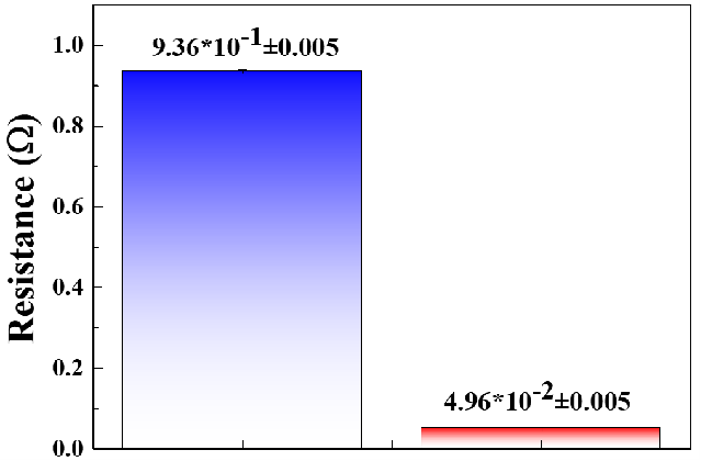
Graphite / YWIT - graphene
Resistance of our graphene is much lower than that of commercial graphite.